
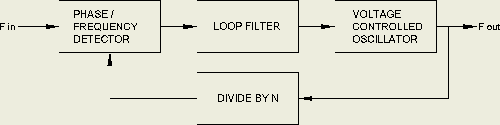
Phase Lock Loops have long been used for clock recovery, fixed frequency multiplication, reducing clock jitter, frequency synthesis, FM modulation / demodulation, and other tasks. The basic PLL consists of a Phase/Frequency Detector, loop filter, and Voltage Controlled Oscillator whose output is fed back to the detector through an optional digital frequency divider. When the loop locks to the input frequency, the output frequency is equal to the input frequency times the divider ratio.
Direct Digital Synthesis circuits have supplanted PLLs in many synthesizer roles but the PLL has the advantages of cost, simplicity, and the ability to maintain constant phase lock to the source. RCA application note ICAN-6101 describes the use of a CD4046 Phase-Locked-Loop IC as the heart of a 3 digit 1KHz to 1MHz synthesizer. Note that for synthesizer applications it is necessary to use the Frequency detector PC2 rather than the simple Phase detector, PC1. The biggest issue with this circuit is that the loop damping factor varies with the square root of the loop gain which is the product of the PFD and VCO gains divided by the division ratio. The PFD gain is in volts per Hz and the VCO gain is in Hz per volt so the loop gain is dimensionless. At high division ratios, i.e. high frequencies, the loop is under damped and is over damped at low frequencies. This is a trace of a standard PLL synthesizer VCO control input switching between 3KHz and 1.024MHz.
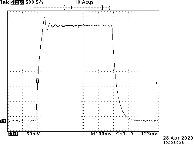
Note that the response at the high frequency end is oscillatory and highly under damped with a settling time of about 200 milliseconds. The low frequency response is highly over damped with a similar settling time. The loop filter constants were chosen to equalize settling times. Improving either degrades the other. This circuit uses a CD74HC4046 for a faster VCO at 5 volts. Unlike the CD4046, the HC4046 VCO has a limited common mode range at the VCOin pin and is normally only capable of a 5 to 1 frequency ratio. To get ratios of 300 to 1 or higher there is a simple workaround.
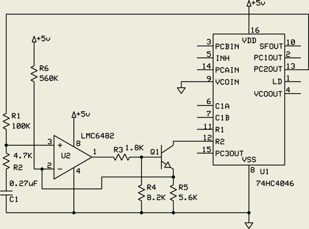
By grounding the VCOin pin and applying the VCO signal as a sinking current source to the frequency offset input the full range of the VCO is available down to essentially zero Hz. R6 raises the low frequency voltage enough to avoid Vos problems with U2. R3 and R4 limit the Q1 common mode range to keep it under the pin 12 bias point.
The RCA application note suggests switching in different loop filter components for different frequency ranges but this doesn’t really fix the problem and is less practical with digital control. Traditional PLL loops have linear VCO gains. This is essential for applications such as FM modulator / demodulators. The main insight here is that the settling time is determined by the loop gain at the target voltage. The gain at other voltages is not relevant. If, as the division ratio increases, the VCO gain could be increased, the two would cancel and the damping factor would be constant, allowing simple loop compensation. The solution is an exponential VCO gain response with a low gain at low frequencies (low VCO input voltage) and high gain at high frequencies.
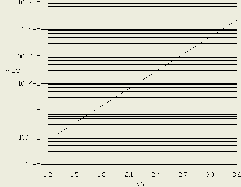
The exponential VCO gain is 4.5KHz per volt at 1KHz and 4.5MHz per volt at 1MHz. One thousand times higher gain at one thousand times the frequency. The question arises as to how to make such a VCO. The obvious solution is to use the Vbe versus Ic relation of silicon junction transistors.
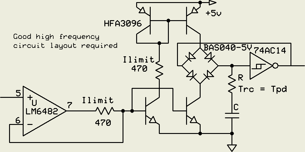
The 470 ohm resistors protect the transistors in case of fault or overload. The diodes are Schottkys. R provides a phase lead to the integrator to compensate for the propagation delay of the Schmitt gate at high frequencies. The matched pair HFA3096 transistors have a gain-bandwidth product of 8GHz which precludes ordinary breadboarding due to parasitic oscillation. A lower speed design was used for this implementation.
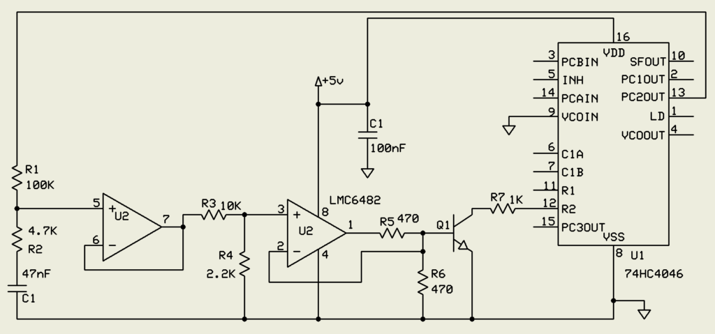
This circuit generated the gain graph above. Q1 is sufficient for the exponential function. As this is only needed for loop stabilization the Vbe temperature coefficient is irrelevant. Note that the loop compensation filter capacitor is one fifth the size of the linear VCO circuit above. The 3KHz to 1.024MHz step response of this circuit is:
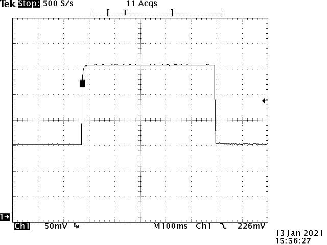
The settling time for both transitions is 900uS and, when zoomed in, both edges are critically damped at high and low frequency.
These kinds of frequency multipliers are useful for synchronous sampling of repetitive signals such as FFT analysis of variable speed rotating equipment at varying resolutions. While FFTs usually are preceded by a windowing function to avoid asynchronous artifacts, these functions broaden spectral lines and reduce the spectrum resolution. With the ability to select FFT sampling rates that are, for instance, 256, 1024, or 4096 times a repetitive signal with a phase locked sampling clock, the requirements for windowing functions can be reduced or even eliminated. This enables trading between resolution and data processing overhead for optimized real-time monitoring.
Please leave any comments using the post in my comments category.