
Electrical switching contacts are not nearly as simple as they seem. Both at make (on) and break (off) they produce various undesirable side effects. Transition times in the nanosecond range can produce unexpected reflections, surges, and arcs in long lines. As the contacts make and break they bounce microscopically causing rapid on and off pulses lasting up to tens of milliseconds. Sliding of the deflecting contact surfaces causes fritting that generates even faster pulses in the microsecond range. At circuit potentials higher than a few volts the bounces produce arcs whose effects range from electromagnetic interference to ignition of explosive atmospheres. This applies to light switches, electromechanical relays, electromechanical timers, and indeed any contact between solid conductors at different potentials.
In our modern solid state low voltage world, contact bounce causes problems with switch interfaces to computers and data gathering systems. If you try to count switch events with an electronic counter it will indicate tens or hundreds of counts for each actuation. A typical computer can read the state of a switch hundreds or thousands of times during the contact bounce time resulting in multiple “clicks” as far as the computer is concerned. The normal solution to this problem is some sort of “debounce” circuit that filters out short transitions and eventually settles to the desired state after 50 milliseconds or so. This works well for mouse buttons or remote TV controls.
Unfortunately this is undesirable for instrumentation, test, or metrology applications, especially multi-channel applications. The delay time will vary from channel to channel and will be affected by the bounce duty cycle. This will make it impossible to accurately determine the time of the initial event closer than a few tens of milliseconds. As an example, in industrial testing it is common to test cam switches at higher than normal speed and correlate the event timing with the cam dwell times which requires very accurate measurements of the initial event timing and sequences.
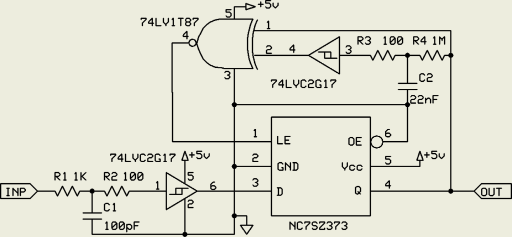
This circuit essentially solves the contact event measurement problem. The switch signal passes through a spike filter and then through a transparent latch. The output of this latch is the cleaned-up input signal and is applied to an exclusive-or gate with a delay on one input. When a transition passes through the latch, the two inputs of the gate are briefly different. This causes the output of the gate to pulse low, holding the state of the latch for the duration of the delayed channel of the exclusive-or gate. This delay is selected to exceed the length of any expected contact bounce but to be shorter than any expected valid signal repetition. At the end of this time the exclusive-or gate unlatches the transparent latch and it reverts to normal. Note that since the contact will have completed its event the output of the latch does not change. As the exclusive-or is not polarity sensitive, this circuit works the same way for rising or falling edges. One consideration is that the data input to must hold steady until the exclusive-or signal is able to latch it. This is about two propagation times or a few nanoseconds for typical logic families and is the purpose of the input spike filter. Its input time constant should be just long enough to guarantee this condition.
This circuit enables contact event measurements with time resolutions of a few nanoseconds.
Please leave comments using the post in my comments category.